microfluidic silicon chip materials fabrication microfluidics device chips elveflow Design of the device and its manufacturing processes can be more challenging for researchers. Although only features in several tens of microns have currently been achieved, this process does offer a number of possibilities. Chiriaco et al. The embossing rollers can be heated and become hot roller embossing. 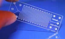 microfluidic functional produce chips rates machines production microfluidics bringing marketplace researchers desktop building Overall, integration of all these techniques and the development of related processes seem to point out a promising direction for the wide usage of microfluidic devices. Song et al. Rapid prototyping of whole-thermoplastic microfluidics with built-in microvalves using laser ablation and thermal fusion bonding. Jo B.-H., Van Lerberghe L.M., Motsegood K.M., Beebe D.J. Ko H.C., Stoykovich M.P., Song J., Malyarchuk V., Choi W.M., Yu C.-J., Geddes III J.B., Xiao J., Wang S., Huang Y., et al. Vinyl chlorides and similar modifications are toxic and difficult to handle. In the case of negative photoresist, exposure to UV light hardens the material whilst the unexposed areas remain soluble and can be washed away during development (Figure 2A). To increase the absorption and reduce the reflection, one can utilise methods such as changing surface finish, applying surface coating, and oxidising the workpiece surface [24]. Investigation on modifying the temperature profile of the embossed film with an aim to improve duplication fidelity by using a conveyer-belt mould is also worth noting [203]. The early SLA systems utilised a point-by-point fashion to scan across each cross section. Ohlander A., Zilio C., Hammerle T., Zelenin S., Klink G., Chiari M., Bock K., Russom A. Genotyping of single nucleotide polymorphisms by melting curve analysis using thin film semi-transparent heaters integrated in a lab-on-foil system. Flexible sensors for chronic wound management. The FIB can engrave or deposit patterns on the workpiece directly from a CAD file. A path: From electroplating through lithographic masks in electronics to LIGA in MEMS. There are requirements for their design as a result of the demoulding process. Experimental study of polymer microlens fabrication using partial-filling hot embossing technique. Moreover, the turnaround time is shorter than for the MEMS process, as there is no mask fabrication and lithography involved; the simplicity is quite attractive for prototyping [39]. Because of the sputtering capability, the FIB is used as a micro- and nanomachining tool in order to modify or machine materials at the micro- and nanoscale. HHS Vulnerability Disclosure, Help LabDisk with complete reagent prestorage for sample-to-answer nucleic acid based detection of respiratory pathogens verified with influenza A H3N2 virus. Electrochemical machining (ECM) utilises the electrochemical dissolution of workpiece in electrolyte upon application of electric potential. Masato D., Sorgato M., Lucchetta G. Analysis of the influence of part thickness on the replication of micro-structured surfaces by injection molding. Figures were created using Biorender and with Figure 2 adapted from a template by Janice Tjan. Unlike an electron microscope, an FIB is inherently destructive to the specimen. ; permission to publish was by next of kin. Ding J., Jiang J., Blanchetire C., Callender C.L.
The possible capability of polymeric microfluidic devices will be almost unlimited. For the direct impact effect, the workpiece is abraded upon direct pounding by the tool through the abrasive particles caught in between the tool and the workpiece. Formed thin sheet-based structures use less materials in contrast to the relatively bulky chip structures formed by hot embossing or injection moulding. Truckenmuller et al. Chien R.-D. Micromolding of biochip devices designed with microchannels. Many hours are usually required to expose a 4 wafer area, and the need of a vacuum chamber limits the size of the workpiece; moreover, the initial capital investment required for an e-beam machine is high. Brittle materials, such as ceramics, silicon, and glass, are generally easier to machine because of the brittle-breakage principle of the method; soft or ductile materials are less efficient because much of the vibration is absorbed elastically or the workpiece is not chipped away easily due to ductility. Mamleyev E.R., Heissler S., Nefedov A., Weidler P.G., Nordin N., Kudryashov V.V., Lnge K., MacKinnon N., Sharma S. Laser-induced hierarchical carbon patterns on polyimide substrates for flexible urea sensors. Fabrication of Microfluidic Reactors and Mixing Studies for Luciferase Detection. Microstructuring of polymer films for sensitive genotyping by real-time PCR on a centrifugal microfluidic platform. Room-temperature and low-pressure nanoimprint lithography. A number of other similar approaches have been demonstrated [93,94,96]. Cavities, holes, channels, and 3D structures are common applications (see Datta et al. Moreover, orientation of polymer chain in substrate is also considered as an effect on the fidelity of hot embossing. They offer product developers the ability to print parts and assemblies made of several materials with different mechanical and physical properties in a single build process.
For replication manufacturing, a mould with micro or nano features is first fabricated; replicates of this master are subsequently moulded. Becker H., Locascio L.E. For the energy-assisted methods, an energy beam of a certain wavelength interacts with the polymer and the effect can be constructive or destructive for polymerisation. Fabrication of large SU-8 mold with high aspect ratio microchannels by UV exposure dose reduction. Weigl B.H., Bardell R., Schulte T., Battrell F., Hayenga J. For ease of discussion, we categorised the methods as mechanical, energy-assisted, and MEMS-based methods [17]. An IR (Infrared) laser was used to pattern graphitic carbonwith induced localised rapid pyrolysison polyimide (Kapton) film and create a flexible urea sensor through both direct urease enzyme immobilisation onto carbon and indirect electrodeposition of an intermediate chitosan before urease immobilisation [139]. microfluidic chip petr tasmania chemistry The volatile by-product is removed by vacuum [54]. microfluidic leak chip resistant fabrication elveflow setup fig courtesy Electronics manufacturing has largely been carried out using rigid printed circuit board (PCB) technologyhaving the advantages of reliability and low costand with increasing interest in use for the development of lab-on-chip systems [223]. All parts are cooled to below the glass transition temperature of the polymer, and the processed polymer is demoulded (see. Piotter V., Hanemann T., Ruprecht R., Hauelt J. Injection molding and related techniques for fabrication of microstructures. Mech. Becker et al. (A) Five-layer split and recombine micromixer.
Shaegh S.A.M., Pourmand A., Nabavinia M., Avci H., Tamayol A., Mostafalu P., Ghavifekr H.B., Aghdam E.N., Dokmeci M.R., Khademhosseini A., et al.
[97,202] devised a discontinuous system which is capable of stopping embossing before the optimal condition is reached. Various studies show that among the prevailing process conditions the following are critical [40,179].
Rapid, low cost prototyping of transdermal devices for personal healthcare monitoring. The interaction between the mould and the polymer is important; low friction is necessary such that the moulded micro-structures and mould are not damaged during the demoulding process. Typically, a laser is used to sinter the media and form the solid. A diamond-coated tool to feed with small depth and slow speed can handle the difficulties, but the wear rate of tools can be high [22]. Review on micro molding of thermoplastic polymers. Chang C.-Y., Yang S.-Y., Chu M.-H. Xia Y., Whitesides G.M. Ro K.W., Lim K., Kim H., Hahn J.H. Higher pressure, temperature of the roller, pre-heating temperature, as well as a slower roller speed help to achieve deeper embossing depths [93,95,198]. Vinyl monomers are those that contain carboncarbon double bonds with the simplest vinyl polymer, polyethylene (PE), formed from the ethylene monomer. Shan et al. Flexible fluidic microchips based on thermoformed and locally modified thin polymer films. Elastomers are weakly crosslinked polymers which change their shape under external force and return to the original shape after the force is removed. Casting is the fabrication process primarily for silicone-based elastomers to mould or to be used as a stamp to create micro- or nanostructures, and is often referred to as soft lithography. Bhavsar S.N., Aravindan S., Rao P.V. The advantage of laser ablation includes its wide acceptance of workpiece materials. These microfluidic devices have shown great potential to reduce cost in manufacturing, consumption of reagents, and time of analysis and to increase device efficiency and portability [1,2,3,4,5]. microfluidics manufacturing Palavesam N., Marin S., Hemmetzberger D., Landesberger C., Bock K., Kutter C. Roll-to-roll processing of film substrates for hybrid integrated flexible electronics.
McGeough J.A., Leu M.C., Rajurkar K.P., De Silva A.K.M., Liu Q. Electroforming Process and Application to Micro/Macro Manufacturing. Mechanical methods are relatively traditional and use tools to remove unnecessary materials. The interactive combination of processes parameters, material properties, and part geometry are yet to be substantially explored and investigated. pmma microfluidic pdms fabricating Variant approach replacing the X-ray lithography with a UV one is also widely used and usually termed as UV-LIGA or modified LIGA. An official website of the United States government. The setup of ECM is similar to that of electroplating, but with the workpiece on the anode and the tool, or the electrode, on the cathode. It is also difficult to predict or detect breakages of the tool because of the small size. Chemical interactions between the materials of the master and the moulded device are also important, and surface treatment is sometimes used for control of these interactions.  Toren P., Smolka M., Haase A., Palfinger U., Nees D., Ruttloff S., Kuna L., Schaude C., Jauk S., Rumpler M., et al. The film is clamped at its edges and heated to the glass transition temperature of the material; the softened material is then stretched against moulds with the assistance of pneumatic or mechanical pressure; the structure is then cooled and demoulded. Most nickel moulds have a thickness of around 50100 m and are attached to the roller by taping, double taping, or clamping.