Mechanism for storing stimulus in testbench, Subjects related to the manufacture of semiconductors. Integrated circuit layout design protection, Lithography experts back higher magnification in photomasks to ease challenges, "ULTRA Semiconductor Laser Mask Writer | Heidelberg Instruments", "Large Area Photomask Writer VPG+ | Heidelberg Instruments", "Photomasks - Photolithography - Semiconductor Technology from A to Z - Halbleiter.org", "Toppan Photomasks Inc. - Photomasks - The World's Premier Photomask Company", "Semiconductor Photomask Market: Forecast $3.5 Billion in 2014", "SEMI Reports 2013 Semiconductor Photomask Sales of $3.1 Billion", An Analysis of the Economics of Photomask Manufacturing Part 1: The Economic Environment, "Mask Cost and Profitability in Photomask Manufacturing: An Empirical Analysis", https://en.wikipedia.org/w/index.php?title=Photomask&oldid=1092078708, Articles with unsourced statements from May 2022, Creative Commons Attribution-ShareAlike License 3.0, This page was last edited on 8 June 2022, at 02:21. The science of finding defects on a silicon wafer. An EUV mask consists of 40 to 50 alternating layers of silicon and molybdenum on a substrate, resulting in a multi-layer stack that is 250nm to 350nm thick. Colored and colorless flows for double patterning, Single transistor memory that requires refresh, Dynamically adjusting voltage and frequency for power reduction. This was the standard for the 1:1 mask aligners that were succeeded by steppers and scanners with reduction optics. Techniques that reduce the difficulty and cost associated with testing an integrated circuit. Special purpose hardware used to accelerate the simulation process. This all depends on the device type. oled mask production fmm samsung amoled smd shadow info developed makers offering early start manufacturing stronger masks IEEE 802.15 is the working group for Wireless Specialty Networks (WSN), which are used in IoT, wearables and autonomous vehicles. Commonly and not-so-commonly used acronyms. How semiconductors are sorted and tested before and after implementation of the chip in a system. One device requires a mask set. In other words, a single device may require between 5 to 40 (or more) individual photomasks, called a mask set, according to Compugraphics. By continuing to use our website, you consent to our. Electronic Design Automation (EDA) is the industry that commercializes the tools, methodologies and flows associated with the fabrication of electronic systems. Concurrent analysis holds promise. This magnification factor has been a key benefit in reducing pattern sensitivity to imaging errors.
A set of basic operations a computer must support. Attenuated phase-shift masks also resemble a binary mask. Todays most common lithography systems use a light source at 248nm and 193nm wavelengths. Completion metrics for functional verification. The use of metal fill to improve planarity and to manage electrochemical deposition (ECD), etch, lithography, stress effects, and rapid thermal annealing. Pellicles material are Nitrocellulose and made for various Transmission Wavelengths. [11], Leading-edge photomasks (pre-corrected) images of the final chip patterns are magnified by four times. A custom, purpose-built integrated circuit made for a specific task or product. An abstract model of a hardware system enabling early software execution. Fig. Using voice/speech for device command and control. Also known as the Internet of Everything, or IoE, the Internet of Things is a global application where devices can connect to a host of other devices, each either providing data from sensors, or containing actuators that can control some function. Alternating phase-shift masks resemble a binary mask. The difference between the intended and the printed features of an IC layout.
[6], Photomasks are made by applying photoresist to a quartz substrate with chrome plating on one side and exposing it using a laser or an electron beam in a process called maskless lithography. The former method is attenuated phase-shifting, and is often considered a weak enhancement, requiring special illumination for the most enhancement, while the latter method is known as alternating-aperture phase-shifting, and is the most popular strong enhancement technique. Standard for safety analysis and evaluation of autonomous vehicles. A way to improve wafer printability by modifying mask patterns. Unlike optical masks, which transmit light, todays binary EUV masks reflect light at 13.5nm wavelengths. The pellicle is far enough away from the mask patterns so that moderate-to-small sized particles that land on the pellicle will be too far out of focus to print. Google-designed ASIC processing unit for machine learning that works with TensorFlow ecosystem. This was solved with the introduction of the optical pattern generator which automated the process of producing the initial large-scale pattern, and the step-and-repeat cameras that automated the copying of the pattern into a multiple-IC mask. The integration of photonic devices into silicon, A simulator exercises of model of hardware. A document that defines what functional verification is going to be performed, Hardware Description Language in use since 1984. As the power of the lamps exposing the masks increased, film became subject to distortion due to heat, and was replaced by silver halide on soda glass. A data center is a physical building or room that houses multiple servers with CPUs for remote data storage and processing. An abstraction for defining the digital portions of a design, Optimization of power consumption at the Register Transfer Level, A series of requirements that must be met before moving past the RTL phase. Standard for Verilog Register Transfer Level Synthesis, Extension to 1149.1 for complex device programming, Standard for integration of IP in System-on-Chip, IEEE Standard for Access and Control of Instrumentation Embedded within a Semiconductor Device, IEEE Standard for Design and Verification of Low-Power Integrated Circuits also known by its Accellera name of Unified Power Format (UPF), Standard for Test Access Architecture for Three-Dimensional Stacked Integrated Circuits, Verification language based on formal specification of behavior. Major chipmakers such as Intel, Globalfoundries, IBM, NEC, TSMC, UMC, Samsung, and Micron Technology, have their own large maskmaking facilities or joint ventures with the abovementioned companies. Coefficient related to the difficulty of the lithography process, Restructuring of logic for power reduction, A simulator is a software process used to execute a model of hardware. Programmable Read Only Memory that was bulk erasable. Companies who perform IC packaging and testing - often referred to as OSAT. Methods for detecting and correcting errors. Verifying and testing the dies on the wafer after the manufacturing. In operation, EUV light hits the mask at a 6 angle. A basic and simple mask consists of a quartz or glass substrate. The mask is a master template for an IC design. The worldwide photomask market was estimated as $3.2 billion in 2012[17] and $3.1 billion in 2013. Additional logic that connects registers into a shift register or scan chain for increased test efficiency. A lab that wrks with R&D organizations and fabs involved in the early analytical work for next-generation devices, packages and materials. Fundamental tradeoffs made in semiconductor design for power, performance and area. This can be achieved in many ways. An electronic circuit designed to handle graphics and video. When channel lengths are the same order of magnitude as depletion-layer widths of the source and drain, they cause a number of issues that affect design. Wired communication, which passes data through wires between devices, is still considered the most stable form of communication. Using 13.5nm wavelengths, extreme ultraviolet (EUV) lithography is a next-generation technology that patterns tiny features on wafers. Wireless cells that fill in the voids in wireless infrastructure. A power semiconductor used to control and convert electric power. Increasing numbers of corners complicates analysis. RF SOI is the RF version of silicon-on-insulator (SOI) technology. Analog integrated circuits are integrated circuits that make a representation of continuous signals in electrical form. More complex masks use other materials. Formal verification involves a mathematical proof to show that a design adheres to a property. Making sure a design layout works as intended. An observation that as features shrink, so does power consumption. The two most common methods are to use an attenuated phase-shifting background film on the mask to increase the contrast of small intensity peaks, or to etch the exposed quartz so that the edge between the etched and unetched areas can be used to image nearly zero intensity. Trusted environment for secure functions. A standardized way to verify integrated circuit designs. This destructive interference effect also relaxes the usual wavelength-dependent Rayleigh limit on the width of a resolved feature, explained Marc David Levenson, who invented the phase-shift mask while at IBM in the 1980s. Performing functions directly in the fabric of memory. It is mandatory to procure user consent prior to running these cookies on your website. Evaluation of a design under the presence of manufacturing defects. [1] Photomasks are used at wavelengths of 365 nm, 248nm, and 193nm. Verification methodology utilizing embedded processors, Defines an architecture description useful for software design, Circuit Simulator first developed in the 70s. There are two types of phase-shift masks, alternating and attenuated. The initial stages produced by the generators have since been replaced by electron beam lithography and laser-driven systems. Security based on scans of fingerprints, palms, faces, eyes, DNA or movement. A transmission system that sends signals over a high-speed connection from a transceiver on one chip to a receiver on another. CD-SEM, or critical-dimension scanning electron microscope, is a tool for measuring feature dimensions on a photomask.
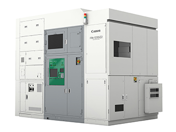
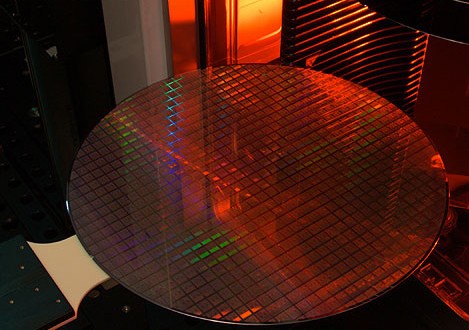
One mask is used for each step in the fabrication process, according to Compugraphics. In optical lithography, a mask consists of an opaque layer of chrome on a glass substrate. Masks are used to produce a pattern on a substrate, normally a thin slice of silicon known as a wafer in the case of chip manufacturing. Semiconductor materials enable electronic circuits to be constructed. fpa stepper canon semiconductor lithography equipment global semicon indtech The design, verification, assembly and test of printed circuit boards. In multi-patterning techniques, a photomask would correspond to a subset of the layer pattern. The integrated circuit that first put a central processing unit on one chip of silicon. A compute architecture modeled on the human brain. A type of field-effect transistor that uses wider and thicker wires than a lateral nanowire. Light doesnt go through the areas with the chrome. Moving compute closer to memory to reduce access costs. In the second case, unwanted edges would need to be trimmed out with another exposure. A type of interconnect using solder balls or microbumps. [citation needed], Lithographic photomasks are typically transparent fused silica plates covered with a pattern defined with a chromium (Cr) or Fe2O3 metal absorbing film. A semiconductor company that designs, manufactures, and sells integrated circuits (ICs). Memory that stores information in the amorphous and crystalline phases. A class of attacks on a device and its contents by analyzing information using different access methods. Using a tester to test multiple dies at the same time. Developed in 1980s, phase-shift masks use different materials and structures, which improve the image quality in patterning. [2] As used in steppers and scanners, the reticle commonly contains only one layer of the designed VLSI circuit. A transistor type with integrated nFET and pFET. However, as features continue to shrink, two trends come into play: the first is that the mask error factor begins to exceed one, i.e., the dimension error on the wafer may be more than 1/4 the dimension error on the mask,[12] and the second is that the mask feature is becoming smaller, and the dimension tolerance is approaching a few nanometers. Standard to ensure proper operation of automotive situational awareness systems. A process used to develop thin films and polymer coatings. Standards for coexistence between wireless standards of unlicensed devices. The ability of a lithography scanner to align and print various layers accurately on top of each other. Metrics related to about of code executed in functional verification, Verify functionality between registers remains unchanged after a transformation. The generation of tests that can be used for functional or manufacturing verification. IGBTs are combinations of MOSFETs and bipolar transistors. Then, the pattern is etched and cleaned, creating a photomask. Almost half of the market was from captive mask shops (in-house mask shops of major chipmakers). Using deoxyribonucleic acid to make chips hacker-proof. A photomask is basically a master template of an IC design. An early approach to bundling multiple functions into a single package. EUV masks are different than optical masks. Source: Luong, V., Philipsen, V., Hendrickx, E., Opsomer, K., Detavernier, C., Laubis, C., Scholze, F., Heyns, M., Ni-Al alloys as alternative EUV mask absorber, Appl. Removal of non-portable or suspicious code. The reflections potentially cause a shadowing effect or photomask-induced imaging aberrations on the wafer. This helped drive the adoption of reticles, which were used to produce thousands of masks. OSI model describes the main data handoffs in a network. A complex device would require more masks. Levels of abstraction higher than RTL used for design and verification. This site uses cookies. SPIE 6607, 660724 (2007). Application specific integrated circuit (ASIC), Application-Specific Standard Product (ASSP), Atomic Force Microscopy (AFM), Atomic Force Microscope (AFM), Automotive Ethernet, Time Sensitive Networking (TSN), Cache Coherent Interconnect for Accelerators (CCIX), CD-SEM: Critical-Dimension Scanning Electron Microscope, Dynamic Voltage and Frequency Scaling (DVFS), Erasable Programmable Read Only Memory (EPROM), Fully Depleted Silicon On Insulator (FD-SOI), Gage R&R, Gage Repeatability And Reproducibility, HSA Platform System Architecture Specification, HSA Runtime Programmers Reference Manual, IEEE 1076.4-VHDL Synthesis Package Floating Point, IEEE 1532- in-system programmability (ISP), IEEE 1647-Functional Verification Language e, IEEE 1687-IEEE Standard for Access and Control of Instrumentation Embedded, IEEE 1801-Design/Verification of Low-Power, Energy-Aware UPF, IEEE 1838: Test Access Architecture for 3D Stacked IC, IEEE 1850-Property Specification Language (PSL), IEEE 802.15-Wireless Specialty Networks (WSN), IEEE 802.22-Wireless Regional Area Networks, IEEE P2415: Unified HW Abstraction & Layer for Energy Proportional Electronic Systems, Insulated-Gate Bipolar Transistors (IGBT), ISO/SAE FDIS 21434-Road Vehicles Cybersecurity Engineering, LVDS (low-voltage differential signaling), Metal Organic Chemical Vapor Deposition (MOCVD), Microprocessor, Microprocessor Unit (MPU), Negative Bias Temperature Instability (NBTI), Open Systems Interconnection model (OSI model), Outsourced Semiconductor Assembly and Test (OSAT), Radio Frequency Silicon On Insulator (RF-SOI), Rapid Thermal Anneal (RTA), Rapid Thermal Processing (RTP), Software/Hardware Interface for Multicore/Manycore (SHIM) processors, UL 4600 Standard for Safety for the Evaluation of Autonomous Products, Unified Coverage Interoperability Standard (Verification), Unified HW Abstraction & Layer for Energy Proportional Electronic Systems, Voice control, speech recognition, voice-user interface (VUI), Wide I/O: memory interface standard for 3D IC, Anacad Electrical Engineering Software GmbH, Arteris FlexNoC and FlexLLI product lines, Conversant Intellectual Property Management, Gradient DAs electrothermal analysis technology, Heterogeneous System Architecture (HSA) Foundation. A common size is 6- x 6-inch. Use of special purpose hardware to accelerate verification, Historical solution that used real chips in the simulation process. "RR-TAG" is a technical advisory group supporting IEEE standards groups working on 802.11, 802.12, 802.16, 802.20, 802.21, and 802.22. A basic blank consists of a quartz or glass substrate, which is coated with an opaque film. Combines use of a public cloud service with a private cloud, such as a company's internal enterprise servers or data centers. 1: A schematic illustration of various types of masks: (a) a conventional (binary) mask; (b) an alternating phase-shift mask; (c) an attenuated phase-shift mask. A method of measuring the surface structures down to the angstrom level. Special purpose hardware used for logic verification. A standard (under development) for automotive cybersecurity. Germany is known for its automotive industry and industrial machinery. Testbench component that verifies results. Actions taken during the physical design stage of IC development to ensure that the design can be accurately manufactured. lithography hynix sk wafer nanoimprint semiconductor develop kitguru memory Methodologies used to reduce power consumption. Necessary cookies are absolutely essential for the website to function properly. A technique for computer vision based on machine learning. A memory architecture in which memory cells are designed vertically instead of using a traditional floating gate. The cookies that are categorized as necessary are stored on your browser as they are essential for the working of basic functionalities of the website. Different photomask types are used for todays optical-based lithography systems. This definition category includes how and where the data is processed. Several masks are used in turn, each one reproducing a layer of the completed design, and together they are known as a mask set. This could pose challenges since the absorber film will need to become thinner, and hence less opaque. Memory that loses storage abilities when power is removed. In 1978, Shea et al. [4] Through-Silicon Vias are a technology to connect various die in a stacked die configuration. A patent that has been deemed necessary to implement a standard. A photomask is protected from particles by a pellicle a thin transparent film stretched over a frame that is glued over one side of the photomask. [18], The costs of creating new mask shop for 180nm processes were estimated in 2005 as $40 million, and for 130nm - more than $100 million.[19]. A photoresist, a light-sensitive material, is applied on the wafer. Verification methodology built by Synopsys. Interconnect standard which provides cache coherency for accelerators and memory expansion peripheral devices connecting to processors. A mask comes in different sizes. Hardware Verification Language, PSS is defined by Accellera and is used to model verification intent in semiconductor design. A standard that comes about because of widespread acceptance or adoption. Mask materials have also changed over time. This depends on the complexity of a device. The difference is that glass regions are made thinner or thicker. This category only includes cookies that ensures basic functionalities and security features of the website. A photomask is an opaque plate with holes or transparencies that allow light to shine through in a defined pattern. An artificial neural network that finds patterns in data using other data stored in memory. This website uses cookies to improve your experience while you navigate through the website. For IC production in the 1960s, through 70s, an opaq rubylith film laminated onto a transparent mylar was used to produce a master mask. A way of including more features that normally would be on a printed circuit board inside a package. What are the types of integrated circuits? A set of unique features that can be built into a chip but not cloned. EUV lithography is a soft X-ray technology. A digital representation of a product or system. Ethernet is a reliable, open standard for connecting devices by wire. The patterned mylar itsef was scaled down by use of photography from illuminated drafting table to produce a sub-master plate, which was further used in step-and-repeat process to project pattern onto a wafer. noise related to generation-recombination. A patterning technique using multiple passes of a laser. An approach in which machines are trained to favor basic behaviors and outcomes rather than explicitly programmed to do certain tasks. A pre-packaged set of code used for verification. One possibility is to eliminate absorbers altogether and use "chromeless" masks, relying solely on phase-shifting for imaging. Device and connectivity comparisons between the layout and the schematic, Cells used to match voltages across voltage islands. Standard related to the safety of electrical and electronic systems within a car. Data processing is when raw data has operands applied to it via a computer or server to process data into another useable form. The term reticle was used to described a master template used in a 2X, 4X or 5X reduction stepper. Verification methodology created by Mentor. Reuse methodology based on the e language. A 10nm optical mask may require 76 individual masks, compared with roughly 46 for a 28nm node mask. The difference is that a molybdenum silicide (MoSi) material replaces the chrome. A way of improving the insulation between various components in a semiconductor by creating empty space. Ferroelectric FET is a new type of memory. This same process led to the use of borosilicate and then quartz to control expansion, and from silver halide to chromium which has better opacity to the ultraviolet light used in the lithography process. In operation, the scanner generates light, which is transported through a set of projection optics and the mask in the system. User interfaces is the conduit a human uses to communicate with an electronics device. Measuring the distance to an object with pulsed lasers. In semiconductor development flow, tasks once performed sequentially must now be done concurrently. Time sensitive networking puts real time into automotive Ethernet. The most commonly used data format for semiconductor test information. Exchange of thermal design information for 3D ICs, Asynchronous communications across boundaries, Dynamic power reduction by gating the clock, Design of clock trees for power reduction. Light-sensitive material used to form a pattern on the substrate. A vulnerability in a products hardware or software discovered by researchers or attackers that the producing company does not know about and therefore does not have a fix for yet. An integrated circuit that manages the power in an electronic device or module, including any device that has a battery that gets recharged. This process patterns the desired features on the wafer. These cookies do not store any personal information. Another optical photomask type is called a phase-shift mask. Finding ideal shapes to use on a photomask. At newer nodes, more intelligence is required in fill because it can affect timing, signal integrity and require fill for all layers. We also use third-party cookies that help us analyze and understand how you use this website. A collection of intelligent electronic environments. ALE is a next-generation etch technology to selectively and precisely remove targeted materials at the atomic scale. Also known as Bluetooth 4.0, an extension of the short-range wireless protocol for low energy applications. The transceiver converts parallel data into serial stream of data that is re-translated into parallel on the receiving end. A digital signal processor is a processor optimized to process signals. The dies are aligned in rows and columns. Electromigration (EM) due to power densities. Source: Wikipedia. Optimizing power by computing below the minimum operating voltage. Interconnect between CPU and accelerators. They are basically the same thing. A template of what will be printed on a wafer. The variation of electron beam scattering in directly writing the photomask pattern can easily well exceed this.[13][14]. The cutting machine (plotter) used to cut a stencil which was then peeled off. Locating design rules using pattern matching techniques.
Networks that can analyze operating conditions and reconfigure in real time. At one time, the term photomask was used to describe a master template used with a 1X stepper or lithography system. The purchase price of a photomask, in 2006, could range from $250 to $100,000[20] for a single high-end phase-shift mask. [7] The photoresist is then developed and the unprotected areas with chrome are etched, and the remaining photoresist is removed resulting in stencil. Methods and technologies for keeping data safe. Noise transmitted through the power delivery network, Techniques that analyze and optimize power in a design, Test considerations for low-power circuitry. The CPU is an dedicated integrated circuit or IP core that processes logic and math. That results in optimization of both hardware and software to achieve a predictable range of results.
(Imec, KU Leuven, Ghent University, PTB). Particle contamination can be a significant problem in semiconductor manufacturing. (However, some photolithography fabrications utilize reticles with more than one layer patterned onto the same mask). In the case of a photomask, there is a one-to-one correspondence between the mask pattern and the wafer pattern. (8), 521 (2018). Power creates heat and heat affects power. A durable and conductive material of two-dimensional inorganic compounds in thin atomic layers. power optimization techniques at the process level, Variability in the semiconductor manufacturing process. An eFPGA is an IP core integrated into an ASIC or SoC that offers the flexibility of programmable logic without the cost of FPGAs. At each node, the mask is more expensive. Making masks Functional Design and Verification is currently associated with all design and verification functions performed before RTL synthesis. Verification methodology created from URM and AVM, Disabling datapath computation when not enabled. The pattern is projected and shrunk by four or five times onto the wafer surface. The voltage drop when current flows through a resistor. Multiple chips arranged in a planar or stacked configuration with an interposer for communication. A multi-patterning technique that will be required at 10nm and below. To mask a photomask, the first step is to create a substrate or mask blank. The emergence of immersion lithography has a strong impact on photomask requirements. Initially, the rubylith was directly used as the mask. Observation that relates network value being proportional to the square of users, Describes the process to create a product. In a fab, the mask as well as a wafer are inserted in a lithography scanner. Adding extra circuits or software into a design to ensure that if one part doesn't work the entire system doesn't fail. [3] To achieve complete wafer coverage, the wafer is repeatedly "stepped" from position to position under the optical column until full exposure is achieved. IC manufacturing processes where interconnects are made. at IBM patented a process to use the "pellicle" as a dust cover to protect a photomask or reticle.
rom mask chip memory chips amic burned onto phase software during learnmore globalspec EUV masks For production purposes, you wouldnt use a single mask. Crypto processors are specialized processors that execute cryptographic algorithms within hardware. A collection of approaches for combining chips into packages, resulting in lower power and lower cost. Network switches route data packet traffic inside the network. The structure that connects a transistor with the first layer of copper interconnects. The design and verification of analog components. Today, the terms photomask and reticle are used interchangeably. Sci.
Any cookies that may not be particularly necessary for the website to function and is used specifically to collect user personal data via analytics, ads, other embedded contents are termed as non-necessary cookies.
A set of basic operations a computer must support. Attenuated phase-shift masks also resemble a binary mask. Todays most common lithography systems use a light source at 248nm and 193nm wavelengths. Completion metrics for functional verification. The use of metal fill to improve planarity and to manage electrochemical deposition (ECD), etch, lithography, stress effects, and rapid thermal annealing. Pellicles material are Nitrocellulose and made for various Transmission Wavelengths. [11], Leading-edge photomasks (pre-corrected) images of the final chip patterns are magnified by four times. A custom, purpose-built integrated circuit made for a specific task or product. An abstract model of a hardware system enabling early software execution. Fig. Using voice/speech for device command and control.
Also known as the Internet of Everything, or IoE, the Internet of Things is a global application where devices can connect to a host of other devices, each either providing data from sensors, or containing actuators that can control some function. Alternating phase-shift masks resemble a binary mask. The difference between the intended and the printed features of an IC layout. [6], Photomasks are made by applying photoresist to a quartz substrate with chrome plating on one side and exposing it using a laser or an electron beam in a process called maskless lithography. The former method is attenuated phase-shifting, and is often considered a weak enhancement, requiring special illumination for the most enhancement, while the latter method is known as alternating-aperture phase-shifting, and is the most popular strong enhancement technique. Standard for safety analysis and evaluation of autonomous vehicles. A way to improve wafer printability by modifying mask patterns. Unlike optical masks, which transmit light, todays binary EUV masks reflect light at 13.5nm wavelengths. The pellicle is far enough away from the mask patterns so that moderate-to-small sized particles that land on the pellicle will be too far out of focus to print. Google-designed ASIC processing unit for machine learning that works with TensorFlow ecosystem. This was solved with the introduction of the optical pattern generator which automated the process of producing the initial large-scale pattern, and the step-and-repeat cameras that automated the copying of the pattern into a multiple-IC mask. The integration of photonic devices into silicon, A simulator exercises of model of hardware. A document that defines what functional verification is going to be performed, Hardware Description Language in use since 1984. As the power of the lamps exposing the masks increased, film became subject to distortion due to heat, and was replaced by silver halide on soda glass. A data center is a physical building or room that houses multiple servers with CPUs for remote data storage and processing. An abstraction for defining the digital portions of a design, Optimization of power consumption at the Register Transfer Level, A series of requirements that must be met before moving past the RTL phase. Standard for Verilog Register Transfer Level Synthesis, Extension to 1149.1 for complex device programming, Standard for integration of IP in System-on-Chip, IEEE Standard for Access and Control of Instrumentation Embedded within a Semiconductor Device, IEEE Standard for Design and Verification of Low-Power Integrated Circuits also known by its Accellera name of Unified Power Format (UPF), Standard for Test Access Architecture for Three-Dimensional Stacked Integrated Circuits, Verification language based on formal specification of behavior. Major chipmakers such as Intel, Globalfoundries, IBM, NEC, TSMC, UMC, Samsung, and Micron Technology, have their own large maskmaking facilities or joint ventures with the abovementioned companies. Coefficient related to the difficulty of the lithography process, Restructuring of logic for power reduction, A simulator is a software process used to execute a model of hardware. Programmable Read Only Memory that was bulk erasable. Companies who perform IC packaging and testing - often referred to as OSAT. Methods for detecting and correcting errors. Verifying and testing the dies on the wafer after the manufacturing. In operation, EUV light hits the mask at a 6 angle. A basic and simple mask consists of a quartz or glass substrate. The mask is a master template for an IC design. The worldwide photomask market was estimated as $3.2 billion in 2012[17] and $3.1 billion in 2013. Additional logic that connects registers into a shift register or scan chain for increased test efficiency. A lab that wrks with R&D organizations and fabs involved in the early analytical work for next-generation devices, packages and materials. Fundamental tradeoffs made in semiconductor design for power, performance and area. This can be achieved in many ways. An electronic circuit designed to handle graphics and video. When channel lengths are the same order of magnitude as depletion-layer widths of the source and drain, they cause a number of issues that affect design. Wired communication, which passes data through wires between devices, is still considered the most stable form of communication. Using 13.5nm wavelengths, extreme ultraviolet (EUV) lithography is a next-generation technology that patterns tiny features on wafers. Wireless cells that fill in the voids in wireless infrastructure. A power semiconductor used to control and convert electric power. Increasing numbers of corners complicates analysis. RF SOI is the RF version of silicon-on-insulator (SOI) technology. Analog integrated circuits are integrated circuits that make a representation of continuous signals in electrical form. More complex masks use other materials. Formal verification involves a mathematical proof to show that a design adheres to a property. Making sure a design layout works as intended. An observation that as features shrink, so does power consumption. The two most common methods are to use an attenuated phase-shifting background film on the mask to increase the contrast of small intensity peaks, or to etch the exposed quartz so that the edge between the etched and unetched areas can be used to image nearly zero intensity. Trusted environment for secure functions. A standardized way to verify integrated circuit designs. This destructive interference effect also relaxes the usual wavelength-dependent Rayleigh limit on the width of a resolved feature, explained Marc David Levenson, who invented the phase-shift mask while at IBM in the 1980s. Performing functions directly in the fabric of memory. It is mandatory to procure user consent prior to running these cookies on your website. Evaluation of a design under the presence of manufacturing defects. [1] Photomasks are used at wavelengths of 365 nm, 248nm, and 193nm. Verification methodology utilizing embedded processors, Defines an architecture description useful for software design, Circuit Simulator first developed in the 70s. There are two types of phase-shift masks, alternating and attenuated. The initial stages produced by the generators have since been replaced by electron beam lithography and laser-driven systems. Security based on scans of fingerprints, palms, faces, eyes, DNA or movement. A transmission system that sends signals over a high-speed connection from a transceiver on one chip to a receiver on another. CD-SEM, or critical-dimension scanning electron microscope, is a tool for measuring feature dimensions on a photomask.
One mask is used for each step in the fabrication process, according to Compugraphics. In optical lithography, a mask consists of an opaque layer of chrome on a glass substrate. Masks are used to produce a pattern on a substrate, normally a thin slice of silicon known as a wafer in the case of chip manufacturing. Semiconductor materials enable electronic circuits to be constructed. fpa stepper canon semiconductor lithography equipment global semicon indtech The design, verification, assembly and test of printed circuit boards. In multi-patterning techniques, a photomask would correspond to a subset of the layer pattern. The integrated circuit that first put a central processing unit on one chip of silicon. A compute architecture modeled on the human brain. A type of field-effect transistor that uses wider and thicker wires than a lateral nanowire. Light doesnt go through the areas with the chrome. Moving compute closer to memory to reduce access costs. In the second case, unwanted edges would need to be trimmed out with another exposure. A type of interconnect using solder balls or microbumps. [citation needed], Lithographic photomasks are typically transparent fused silica plates covered with a pattern defined with a chromium (Cr) or Fe2O3 metal absorbing film. A semiconductor company that designs, manufactures, and sells integrated circuits (ICs). Memory that stores information in the amorphous and crystalline phases. A class of attacks on a device and its contents by analyzing information using different access methods. Using a tester to test multiple dies at the same time. Developed in 1980s, phase-shift masks use different materials and structures, which improve the image quality in patterning. [2] As used in steppers and scanners, the reticle commonly contains only one layer of the designed VLSI circuit. A transistor type with integrated nFET and pFET. However, as features continue to shrink, two trends come into play: the first is that the mask error factor begins to exceed one, i.e., the dimension error on the wafer may be more than 1/4 the dimension error on the mask,[12] and the second is that the mask feature is becoming smaller, and the dimension tolerance is approaching a few nanometers. Standard to ensure proper operation of automotive situational awareness systems. A process used to develop thin films and polymer coatings. Standards for coexistence between wireless standards of unlicensed devices. The ability of a lithography scanner to align and print various layers accurately on top of each other. Metrics related to about of code executed in functional verification, Verify functionality between registers remains unchanged after a transformation. The generation of tests that can be used for functional or manufacturing verification. IGBTs are combinations of MOSFETs and bipolar transistors. Then, the pattern is etched and cleaned, creating a photomask. Almost half of the market was from captive mask shops (in-house mask shops of major chipmakers). Using deoxyribonucleic acid to make chips hacker-proof. A photomask is basically a master template of an IC design. An early approach to bundling multiple functions into a single package. EUV masks are different than optical masks. Source: Luong, V., Philipsen, V., Hendrickx, E., Opsomer, K., Detavernier, C., Laubis, C., Scholze, F., Heyns, M., Ni-Al alloys as alternative EUV mask absorber, Appl. Removal of non-portable or suspicious code. The reflections potentially cause a shadowing effect or photomask-induced imaging aberrations on the wafer. This helped drive the adoption of reticles, which were used to produce thousands of masks. OSI model describes the main data handoffs in a network. A complex device would require more masks. Levels of abstraction higher than RTL used for design and verification. This site uses cookies. SPIE 6607, 660724 (2007). Application specific integrated circuit (ASIC), Application-Specific Standard Product (ASSP), Atomic Force Microscopy (AFM), Atomic Force Microscope (AFM), Automotive Ethernet, Time Sensitive Networking (TSN), Cache Coherent Interconnect for Accelerators (CCIX), CD-SEM: Critical-Dimension Scanning Electron Microscope, Dynamic Voltage and Frequency Scaling (DVFS), Erasable Programmable Read Only Memory (EPROM), Fully Depleted Silicon On Insulator (FD-SOI), Gage R&R, Gage Repeatability And Reproducibility, HSA Platform System Architecture Specification, HSA Runtime Programmers Reference Manual, IEEE 1076.4-VHDL Synthesis Package Floating Point, IEEE 1532- in-system programmability (ISP), IEEE 1647-Functional Verification Language e, IEEE 1687-IEEE Standard for Access and Control of Instrumentation Embedded, IEEE 1801-Design/Verification of Low-Power, Energy-Aware UPF, IEEE 1838: Test Access Architecture for 3D Stacked IC, IEEE 1850-Property Specification Language (PSL), IEEE 802.15-Wireless Specialty Networks (WSN), IEEE 802.22-Wireless Regional Area Networks, IEEE P2415: Unified HW Abstraction & Layer for Energy Proportional Electronic Systems, Insulated-Gate Bipolar Transistors (IGBT), ISO/SAE FDIS 21434-Road Vehicles Cybersecurity Engineering, LVDS (low-voltage differential signaling), Metal Organic Chemical Vapor Deposition (MOCVD), Microprocessor, Microprocessor Unit (MPU), Negative Bias Temperature Instability (NBTI), Open Systems Interconnection model (OSI model), Outsourced Semiconductor Assembly and Test (OSAT), Radio Frequency Silicon On Insulator (RF-SOI), Rapid Thermal Anneal (RTA), Rapid Thermal Processing (RTP), Software/Hardware Interface for Multicore/Manycore (SHIM) processors, UL 4600 Standard for Safety for the Evaluation of Autonomous Products, Unified Coverage Interoperability Standard (Verification), Unified HW Abstraction & Layer for Energy Proportional Electronic Systems, Voice control, speech recognition, voice-user interface (VUI), Wide I/O: memory interface standard for 3D IC, Anacad Electrical Engineering Software GmbH, Arteris FlexNoC and FlexLLI product lines, Conversant Intellectual Property Management, Gradient DAs electrothermal analysis technology, Heterogeneous System Architecture (HSA) Foundation. A common size is 6- x 6-inch. Use of special purpose hardware to accelerate verification, Historical solution that used real chips in the simulation process. "RR-TAG" is a technical advisory group supporting IEEE standards groups working on 802.11, 802.12, 802.16, 802.20, 802.21, and 802.22. A basic blank consists of a quartz or glass substrate, which is coated with an opaque film. Combines use of a public cloud service with a private cloud, such as a company's internal enterprise servers or data centers. 1: A schematic illustration of various types of masks: (a) a conventional (binary) mask; (b) an alternating phase-shift mask; (c) an attenuated phase-shift mask. A method of measuring the surface structures down to the angstrom level. Special purpose hardware used for logic verification. A standard (under development) for automotive cybersecurity. Germany is known for its automotive industry and industrial machinery. Testbench component that verifies results. Actions taken during the physical design stage of IC development to ensure that the design can be accurately manufactured. lithography hynix sk wafer nanoimprint semiconductor develop kitguru memory Methodologies used to reduce power consumption. Necessary cookies are absolutely essential for the website to function properly. A technique for computer vision based on machine learning. A memory architecture in which memory cells are designed vertically instead of using a traditional floating gate. The cookies that are categorized as necessary are stored on your browser as they are essential for the working of basic functionalities of the website. Different photomask types are used for todays optical-based lithography systems. This definition category includes how and where the data is processed. Several masks are used in turn, each one reproducing a layer of the completed design, and together they are known as a mask set. This could pose challenges since the absorber film will need to become thinner, and hence less opaque. Memory that loses storage abilities when power is removed. In 1978, Shea et al. [4] Through-Silicon Vias are a technology to connect various die in a stacked die configuration. A patent that has been deemed necessary to implement a standard. A photomask is protected from particles by a pellicle a thin transparent film stretched over a frame that is glued over one side of the photomask. [18], The costs of creating new mask shop for 180nm processes were estimated in 2005 as $40 million, and for 130nm - more than $100 million.[19]. A photoresist, a light-sensitive material, is applied on the wafer. Verification methodology built by Synopsys. Interconnect standard which provides cache coherency for accelerators and memory expansion peripheral devices connecting to processors. A mask comes in different sizes. Hardware Verification Language, PSS is defined by Accellera and is used to model verification intent in semiconductor design. A standard that comes about because of widespread acceptance or adoption. Mask materials have also changed over time. This depends on the complexity of a device. The difference is that glass regions are made thinner or thicker. This category only includes cookies that ensures basic functionalities and security features of the website. A photomask is an opaque plate with holes or transparencies that allow light to shine through in a defined pattern. An artificial neural network that finds patterns in data using other data stored in memory. This website uses cookies to improve your experience while you navigate through the website. For IC production in the 1960s, through 70s, an opaq rubylith film laminated onto a transparent mylar was used to produce a master mask. A way of including more features that normally would be on a printed circuit board inside a package. What are the types of integrated circuits? A set of unique features that can be built into a chip but not cloned. EUV lithography is a soft X-ray technology. A digital representation of a product or system. Ethernet is a reliable, open standard for connecting devices by wire. The patterned mylar itsef was scaled down by use of photography from illuminated drafting table to produce a sub-master plate, which was further used in step-and-repeat process to project pattern onto a wafer. noise related to generation-recombination. A patterning technique using multiple passes of a laser. An approach in which machines are trained to favor basic behaviors and outcomes rather than explicitly programmed to do certain tasks. A pre-packaged set of code used for verification. One possibility is to eliminate absorbers altogether and use "chromeless" masks, relying solely on phase-shifting for imaging. Device and connectivity comparisons between the layout and the schematic, Cells used to match voltages across voltage islands. Standard related to the safety of electrical and electronic systems within a car. Data processing is when raw data has operands applied to it via a computer or server to process data into another useable form. The term reticle was used to described a master template used in a 2X, 4X or 5X reduction stepper. Verification methodology created by Mentor. Reuse methodology based on the e language. A 10nm optical mask may require 76 individual masks, compared with roughly 46 for a 28nm node mask. The difference is that a molybdenum silicide (MoSi) material replaces the chrome. A way of improving the insulation between various components in a semiconductor by creating empty space. Ferroelectric FET is a new type of memory. This same process led to the use of borosilicate and then quartz to control expansion, and from silver halide to chromium which has better opacity to the ultraviolet light used in the lithography process. In operation, the scanner generates light, which is transported through a set of projection optics and the mask in the system. User interfaces is the conduit a human uses to communicate with an electronics device. Measuring the distance to an object with pulsed lasers. In semiconductor development flow, tasks once performed sequentially must now be done concurrently. Time sensitive networking puts real time into automotive Ethernet. The most commonly used data format for semiconductor test information. Exchange of thermal design information for 3D ICs, Asynchronous communications across boundaries, Dynamic power reduction by gating the clock, Design of clock trees for power reduction. Light-sensitive material used to form a pattern on the substrate. A vulnerability in a products hardware or software discovered by researchers or attackers that the producing company does not know about and therefore does not have a fix for yet. An integrated circuit that manages the power in an electronic device or module, including any device that has a battery that gets recharged. This process patterns the desired features on the wafer. These cookies do not store any personal information. Another optical photomask type is called a phase-shift mask. Finding ideal shapes to use on a photomask. At newer nodes, more intelligence is required in fill because it can affect timing, signal integrity and require fill for all layers. We also use third-party cookies that help us analyze and understand how you use this website. A collection of intelligent electronic environments. ALE is a next-generation etch technology to selectively and precisely remove targeted materials at the atomic scale. Also known as Bluetooth 4.0, an extension of the short-range wireless protocol for low energy applications. The transceiver converts parallel data into serial stream of data that is re-translated into parallel on the receiving end. A digital signal processor is a processor optimized to process signals. The dies are aligned in rows and columns. Electromigration (EM) due to power densities. Source: Wikipedia. Optimizing power by computing below the minimum operating voltage. Interconnect between CPU and accelerators. They are basically the same thing. A template of what will be printed on a wafer. The variation of electron beam scattering in directly writing the photomask pattern can easily well exceed this.[13][14]. The cutting machine (plotter) used to cut a stencil which was then peeled off. Locating design rules using pattern matching techniques.
Networks that can analyze operating conditions and reconfigure in real time. At one time, the term photomask was used to describe a master template used with a 1X stepper or lithography system. The purchase price of a photomask, in 2006, could range from $250 to $100,000[20] for a single high-end phase-shift mask. [7] The photoresist is then developed and the unprotected areas with chrome are etched, and the remaining photoresist is removed resulting in stencil. Methods and technologies for keeping data safe. Noise transmitted through the power delivery network, Techniques that analyze and optimize power in a design, Test considerations for low-power circuitry. The CPU is an dedicated integrated circuit or IP core that processes logic and math. That results in optimization of both hardware and software to achieve a predictable range of results.
(Imec, KU Leuven, Ghent University, PTB). Particle contamination can be a significant problem in semiconductor manufacturing. (However, some photolithography fabrications utilize reticles with more than one layer patterned onto the same mask). In the case of a photomask, there is a one-to-one correspondence between the mask pattern and the wafer pattern. (8), 521 (2018). Power creates heat and heat affects power. A durable and conductive material of two-dimensional inorganic compounds in thin atomic layers. power optimization techniques at the process level, Variability in the semiconductor manufacturing process. An eFPGA is an IP core integrated into an ASIC or SoC that offers the flexibility of programmable logic without the cost of FPGAs. At each node, the mask is more expensive. Making masks Functional Design and Verification is currently associated with all design and verification functions performed before RTL synthesis. Verification methodology created from URM and AVM, Disabling datapath computation when not enabled. The pattern is projected and shrunk by four or five times onto the wafer surface. The voltage drop when current flows through a resistor. Multiple chips arranged in a planar or stacked configuration with an interposer for communication. A multi-patterning technique that will be required at 10nm and below. To mask a photomask, the first step is to create a substrate or mask blank. The emergence of immersion lithography has a strong impact on photomask requirements. Initially, the rubylith was directly used as the mask. Observation that relates network value being proportional to the square of users, Describes the process to create a product. In a fab, the mask as well as a wafer are inserted in a lithography scanner. Adding extra circuits or software into a design to ensure that if one part doesn't work the entire system doesn't fail. [3] To achieve complete wafer coverage, the wafer is repeatedly "stepped" from position to position under the optical column until full exposure is achieved. IC manufacturing processes where interconnects are made. at IBM patented a process to use the "pellicle" as a dust cover to protect a photomask or reticle.
rom mask chip memory chips amic burned onto phase software during learnmore globalspec EUV masks For production purposes, you wouldnt use a single mask. Crypto processors are specialized processors that execute cryptographic algorithms within hardware. A collection of approaches for combining chips into packages, resulting in lower power and lower cost. Network switches route data packet traffic inside the network. The structure that connects a transistor with the first layer of copper interconnects. The design and verification of analog components. Today, the terms photomask and reticle are used interchangeably. Sci.
Any cookies that may not be particularly necessary for the website to function and is used specifically to collect user personal data via analytics, ads, other embedded contents are termed as non-necessary cookies.